This marks the final ‘Phase 3’ of my project to build a turnkey MIDI processor. The processor solves a specific problem I had in my home MIDI setup where two pieces of equipment were not talking to each other (see here for a description and analysis of the problem). Of course, the firmware on the device could be adapted to do any other kind of processing.
I'll be working off the breadboard-based prototype to construct a finished PCB.
Disclaimer: any mention of commercial products and services isn't intended as an endorsement: I'm really just documenting my personal experience.
In a previous project, I'd used the EAGLE EDA software; here I decided to try KiCAD instead. I'm not against commercial software in principle, I was just curious to give the open-source alternative a try and see how it stacked up. To get myself up to speed quickly, I used O'Reilly Safari's online course KiCAD Like a Pro.
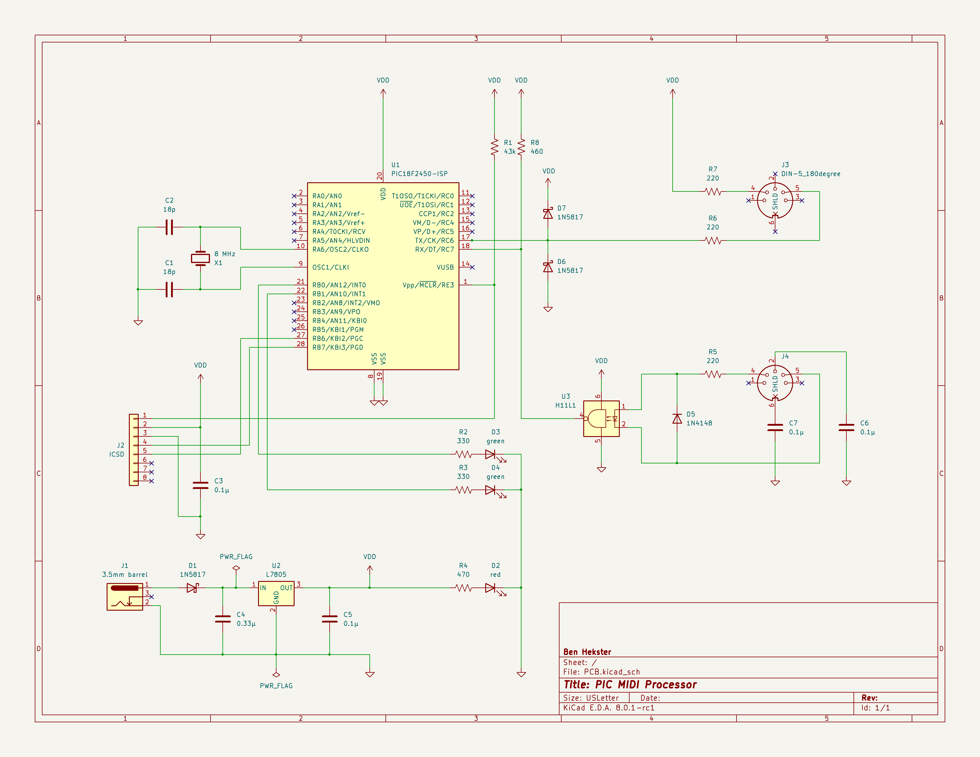
The first step was to create the schematic from the paper version. I also verified the CAD schematic as I disassembled the breadboard prototype. The CAD schematic is more rigorous in that it forces you to explicitly mark unconnected device pins, and mark power lines with ‘power flags’.
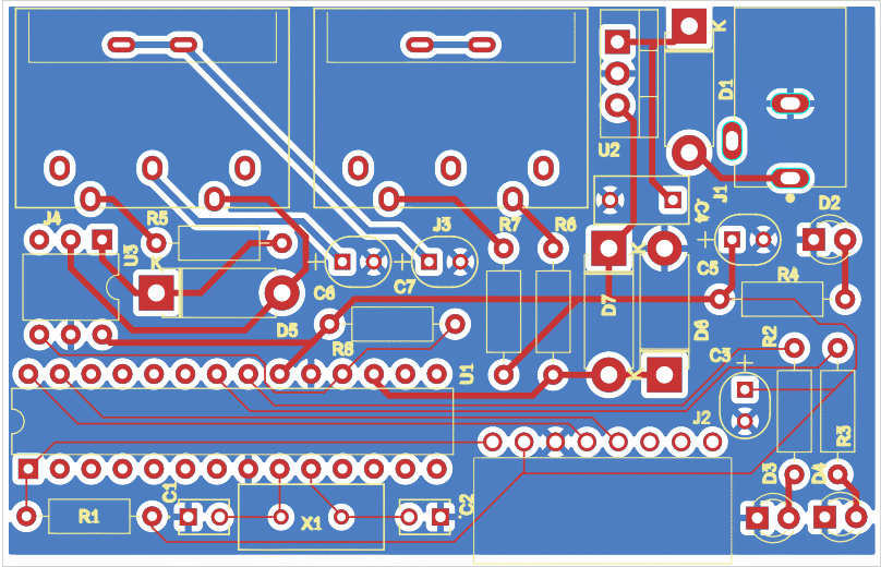
Next comes the actual PCB layout. Most of the components had footprints available in the KiCAD library. For those that didn't I was able to download footprints from UltraLibrarian; these seem to be contributed by the community. For some components (passive) the offering is overwhelming and it does take a little time to pick the most appropriate one.
Optimal placement seems to me still to be mostly intuition, though I did apply some logical constraints: I placed the user connectors (power and DIN) on one side of the board, and the programmer (ICSD) connector on the opposite side. I kept the oscillator close to the microcontroller. Used the rear side as a ground plane.
I found some design guidance online, suggesting using 20 mil trace width for my ‘higher current’ lines (VDD power supply and MIDI signaling), although on this board “high” is still only something on the order of 20 mA. Two online trace width calculators suggested widths that were orders of magnitude less. Since PCB space was not an issue I decided not to take any chances and use the written guidelines. I made a note to myself to measure the voltage drop on one of the power lines to verify.
KiCAD supports assigning lines to ‘net classes’, so theoretically we should be able to have it automatically pick the appropriate trace width. In practice net classes don't exactly solve the problem because some power lines don't actually carry ‘power current’ (like those to pull-up resistors). In some parts of the PCB being able to use a narrower trace width made a difference; so I did this manually.
I've used OSH Park in the past and liked the results. One nice thing is that you can upload the KiCAD project directly; there is no longer any need to export the project as ‘Gerber files’ first.
The batch of three PCBs (the minimum order) arrived about two weeks after placing the order. I started soldering with the small components first, working my way up to the largest ones: the DIN connectors. It was at that point that I realized I'd made two critical mistakes:
Also, I made one mistake in assembly and oriented the LEDs the wrong way. In my haste I remembered the long lead as being ‘special’ in the same way that the stripe on a diode is ‘special’, and associated it with the cathode. This isn't a catastrophic error, of course, because I could re-solder them in the correct orientation. But by slowing down just a bit during assembly I wouldn't have made the mistake in the first place. Some of the generic diode and resistor footprints I used were for higher-power versions and bigger than they needed to be.
On the bright side, I was able to program the device through the ICSP connector, so I knew I was on the right track.
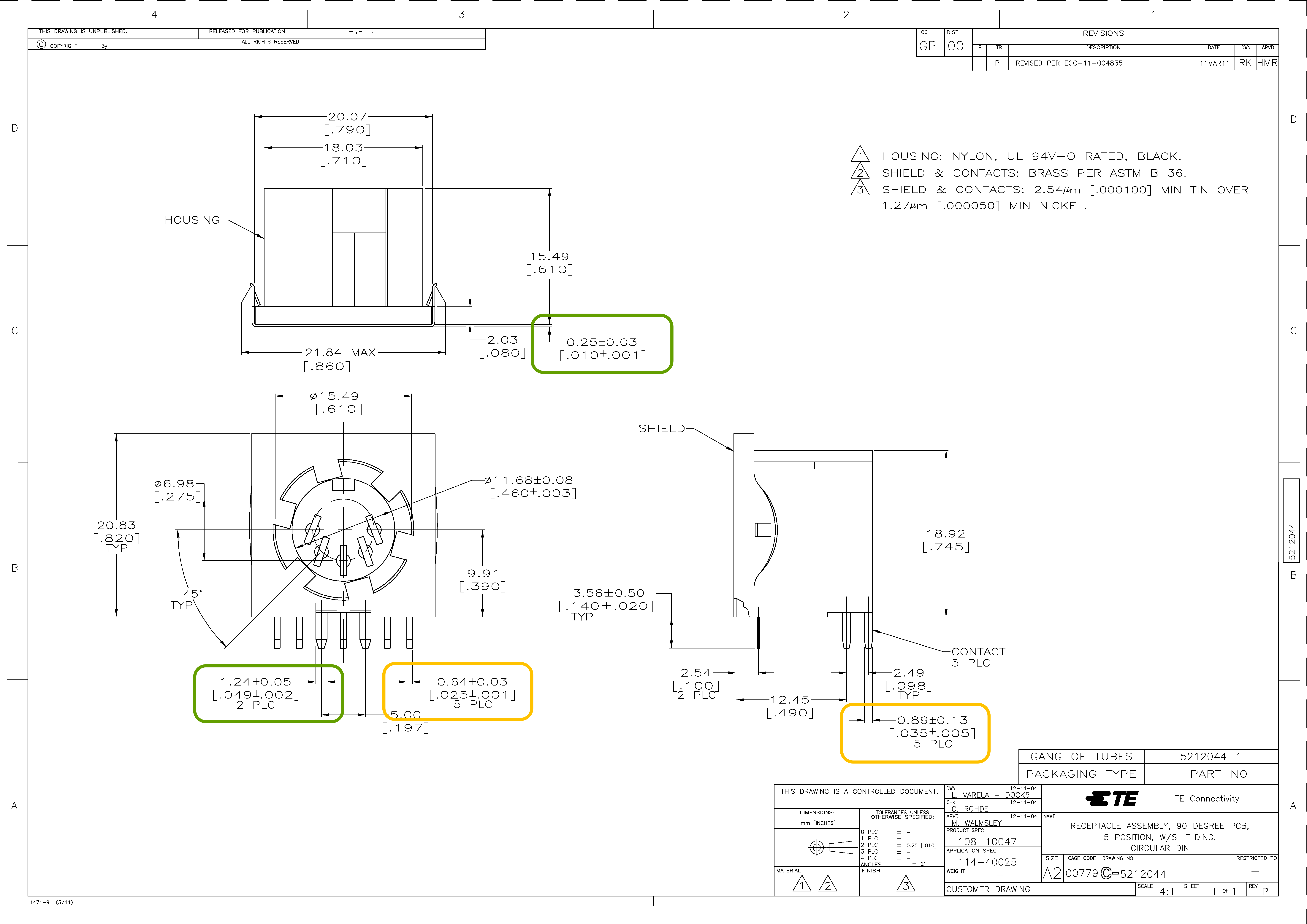
I modified the DIN connector footprint to have the correct drill sizes matching the pin dimensions from the data sheet; and to have a visual indication in the footprint of the connector side. Even though the appears to be unusual, I opted for oval instead of purely round hole sizes because the ‘shield’ pins of the connector are elongated and a round hole would have left an enormous gap. I used the maximum length and width and added the customary 6 mil (≈ 0.15 mm) tolerance.
With these changes, all the parts now fit (although the DIN connector was still quite snug) and the finished product works.
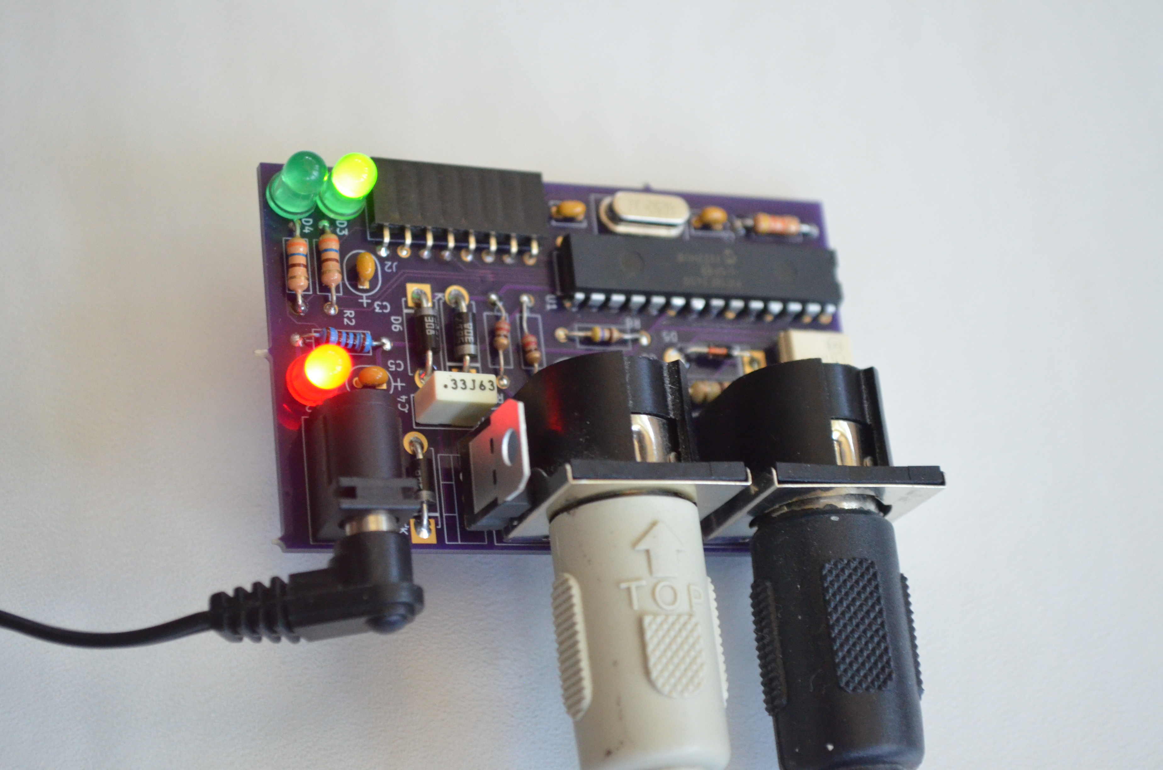
The firmware was unchanged from the breadboard-based prototype and can be found on GitHub in the PIC-MIDI-Processor repository. In the video, for testing and timing purposes, the right green LED blinks at a steady rate of once per second. The left-hand green LED indicates when the device detects we are in ‘play’ mode. The red LED is the power indicator.
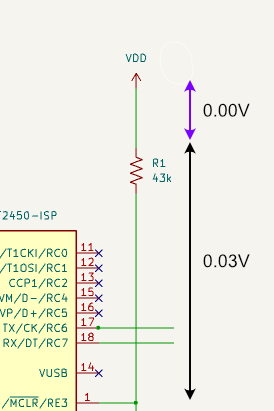
I wanted to convince myself that 20 mil and 6 mil traces don't actually impose unwarranted resistance; in fact, I found no measurable voltage drop across the longest VDD trace (partially carrying supply current).
Incidentally, I also measured a drop of 0.03 V over R1, implying a current of 0.7 μA; this agrees with the data sheet specification (D061) of ±1 μA maximum.
Constructing hardware is not the same as writing software. You have to slow down and work carefully because the cost (time and money) of correcting mistakes is much higher than in programming. Measure twice and cut once! On the other hand, I'm not building a space probe either, so accept that I'll make mistakes and learn along the way.
Fit all components before starting to solder. This would have prevented me from re-buying all the components (through in this case they only cost about $10)
Verify footprints. Especially those from unknown sources. Make sure footprints indicate the connector side. For generic components, don't pick footprints that are unnecessarily large (or, obviously, too small).
Check component orientations. Connectors during PCB design; components during assembly.
Enclosure. Obviously a proper finished product should have a case; maybe the next project.
Additional observations. KiCAD performed excellently on this small product. It's been a while since I used EAGLE so my recollection on how it worked isn't crystal clear, but if I had to choose again I think I'd probably pick KiCAD.
All pages under this domain © Copyright 1999-2024 by: Ben Hekster